Vlsi physical graph partitioning metal layer advertisements contact Electric vlsi tutorial Vlsi flow basics
CMOS Layout Design: Introduction |VLSI Concepts
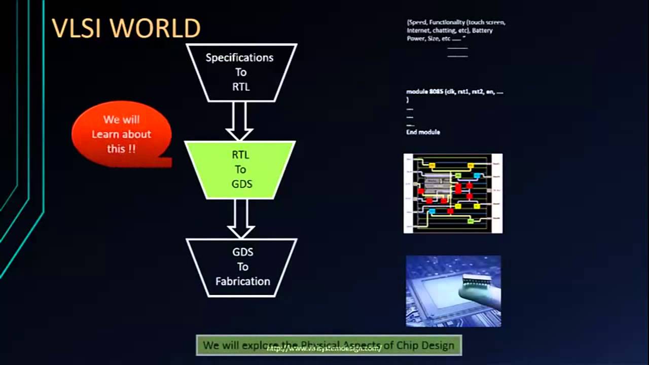
Solved using electric vlsi draw the schematic for a 2:1 Steps in the vlsi circuit design flow [86] Explain the vlsi design flow
Vlsi circuit and system design
Vlsi diagrams nmos daigram jceVlsi analog example short description Cycle de conception vlsi – stacklimaPatent us5659362.
Diagram stick layout path euler vlsi partAdvanced vlsi design What is the function of stick diagram in integrated circuit layout designPatents compression.
Vlsi: steps involved in vlsi design
Introduction to vlsiVlsi overview flow diagram : r/vlsiupdates22 Klmh vlsi physical design from graph partitioningVlsi full form: very large scale integration.
Solved using electric vlsi draw the schematic for anIntroduction to vlsi system design Vlsi cmos synchronous counter project bit 250nm final comments eceFigure 1 from schematic driven layout for the custom vlsi design.

Schematic vlsi compatible process flow diagram for fabrication of our
Diagrams vlsiPrinciples of vlsi design Vlsi process ece advanced slides jimp unm intro c1 edu principlesCmos layout design: introduction |vlsi concepts.
Vlsi process intro ece principles advanced unm jimp slides c1 eduArt of layout – euler’s path and stick diagram – part 1 – vlsi system Vlsi circuit design processVlsi design flow.

Analog vlsi design
Vlsi flow introduction simplified figSketch a transistor-level schematic for a cmos 4-input nor g My final project for vlsi: a 4-bit synchronous counter in 250nm cmosVlsi basics: vlsi design flow.
Vlsi system introductionVlsi schematic compatible quantum How to draw vlsi stick diagrams ?4 bits multiplier design in electric vlsi with vhdl built layout.

Schematic vlsi compatible process flow diagram for fabrication of our
Vlsi schematic compatibleStick vlsi diagram layout circuit integrated system function Solved using electric vlsi draw the schematic for a 2:1Stick-diagrams (2) vlsi.
.


VLSI circuit design process
![Steps in the VLSI Circuit Design Flow [86] | Download Scientific Diagram](https://i2.wp.com/www.researchgate.net/publication/363889257/figure/fig1/AS:11431281086771580@1664335251480/Steps-in-the-VLSI-Circuit-Design-Flow-86.jpg)
Steps in the VLSI Circuit Design Flow [86] | Download Scientific Diagram

4 Bits Multiplier Design in Electric VLSI with VHDL Built Layout

Principles of VLSI Design

Solved Using ELECTRIC VLSI Draw the schematic for an | Chegg.com

KLMH VLSI Physical Design From Graph Partitioning

Patent US5659362 - VLSI circuit structure for implementing JPEG image